Tag Archives: Overclocking

Overclocking a Tanzania

The Tanzania and Tanzania II logic boards were designed by Apple and mainly used by clone makers in machines such as Motorola’s StarMax series of computers. Apple released their own budget “clone” style computer in the form of the Power Macintosh 4400 (the 7220 in some markets).
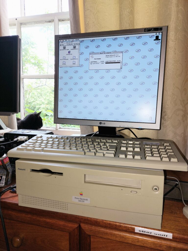
My Power Macintosh 4400/200

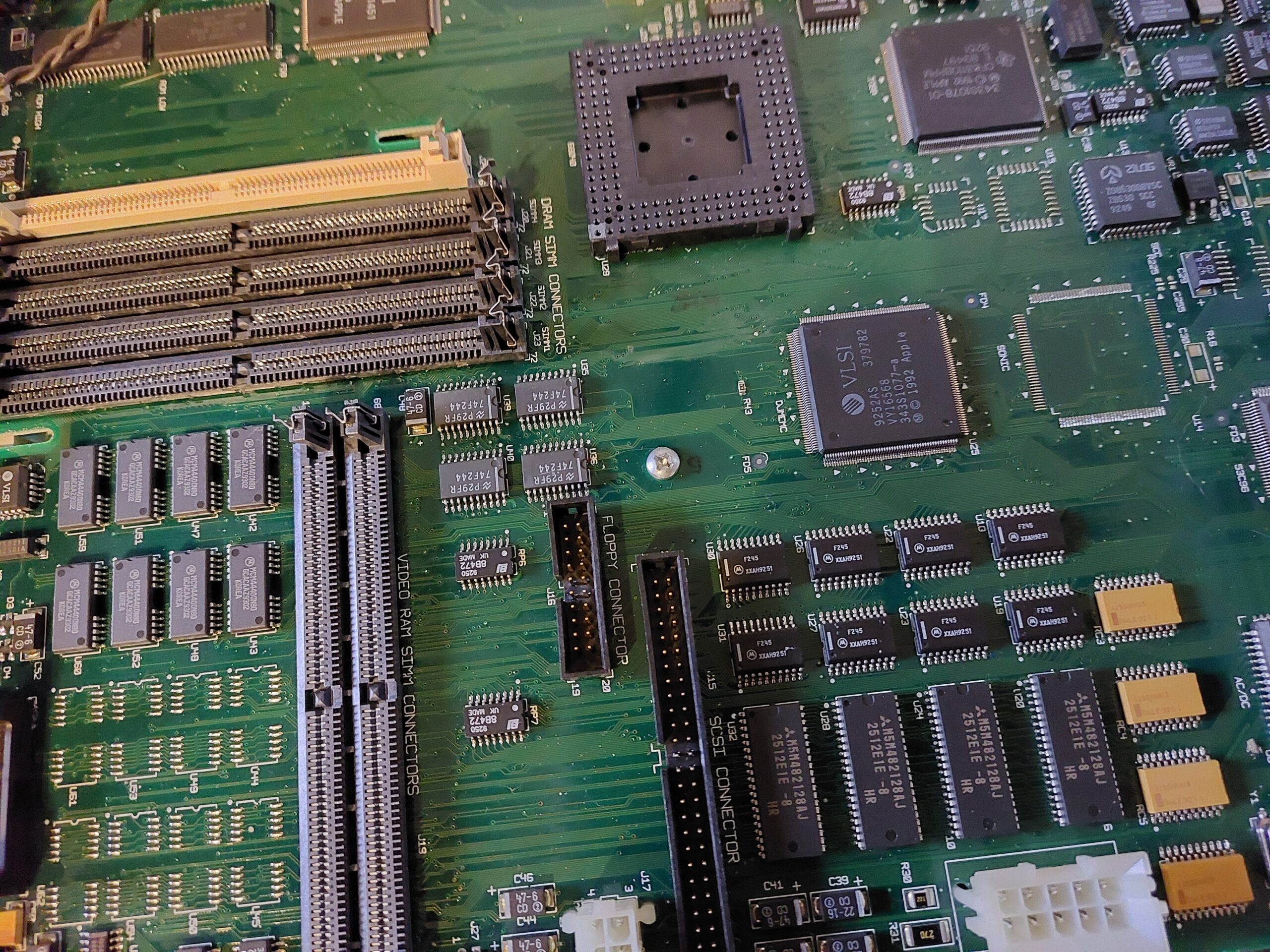
Tanzania based machines came in a verity of configurations with various speeds and a mixture of 603 and 604 family CPUs. What is interesting though is that Motorola variants have the PLL strap settings detailed on the silkscreen! The PLL strap options are what sets the multiplier for the CPU clock speed.
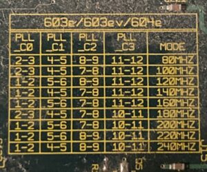
Silkscreen CPU Speed Table (thankyou to the unknown source, friend of a friend of a friend)

Note that the speeds shown in the “Mode” column are from a 40MHz bus machine. If you have a Tanzania II with a 50MHz bus, scale all of those speeds by multiplying them by 1.25 to get the equivalent speed for a 50MHz bus computer.

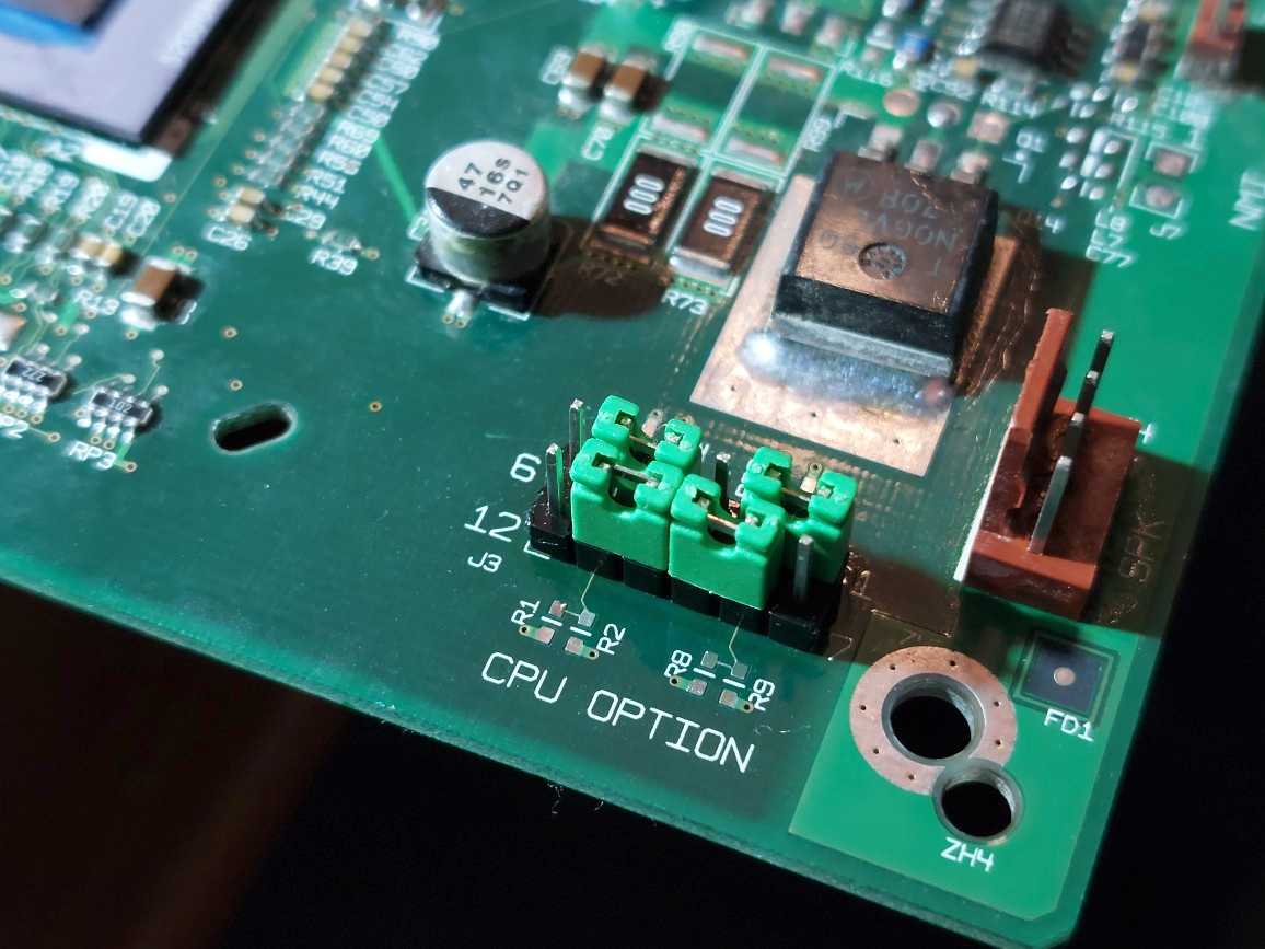
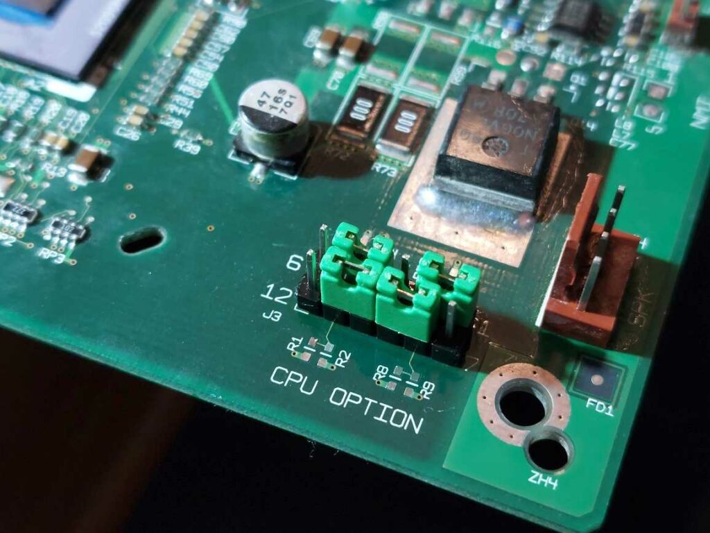
The numbers correspond to the pin numbers on the 12 pin header labelled “CPU Option” in the corner of the board closest to the CPU. By default the header is unpopulated and the clock speed is set by four pull up / pull down resistors on four of eight available positions around the header.
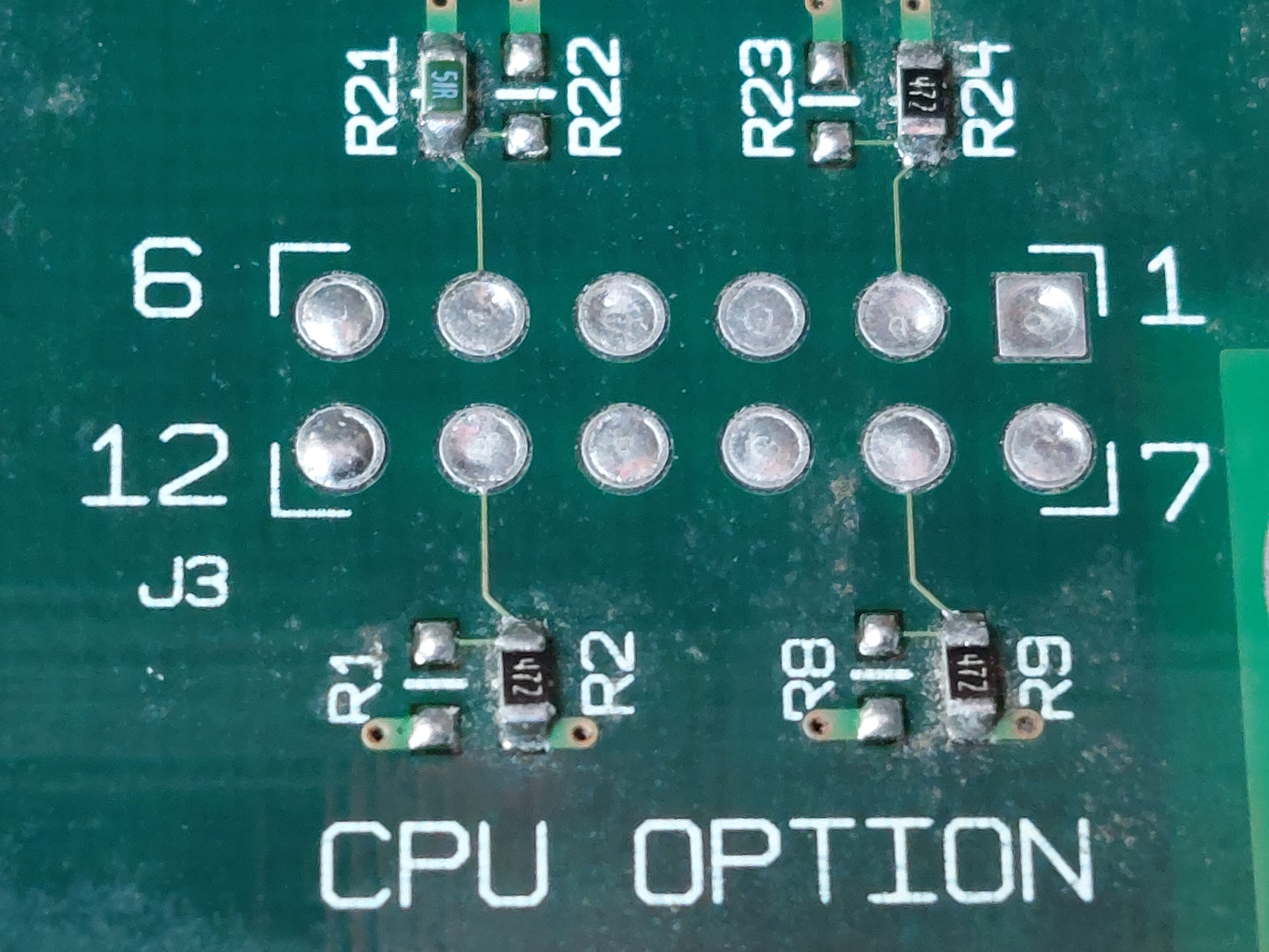
CPU Option Header Showing Default Resistors for 200MHz (Click to View)

The pin numbering can be see around the footprint, and then populating R24 and not R23 is the equivalent of jumpering pins 1+2, while populating R23 and not R24 is equivalent to jumpering pins 2+3. This pattern repeats for pins 4 to 6 with resistors R21 & R22, 7 to 9 with R8 & R9, and lastly 10 to 12 with R1 & R2.

Each set of three pins can be thought of as a toggle switch, for example if you jumper 1+2 together you get one setting, and if you jumper 2+3 together, you get the other.

The resistors set the default and should be removed before jumpering or bridging the corresponding appropriate pairs in the 12 pin header (especially in the case of 51 ohm resistors). Never bridge all three pins in a set of three within the header or you will cause a short and possibly cause damage. Ideally, fit a pin header and use jumpers to change settings. You could even wire in a single pole double throw switch to each set of pins.

Target Speeds

Generally, I’ve found that most processors in various computers (but not all) overclock happily by 20% (I’m not specifically talking about Tanzania based computers, but vintage computers in general). Higher speeds might be achievable, but this is my personal rule of thumb for a ‘more likely than not’ stable overclock. This means that if you have a 160MHz machine, you can likely achieve the 180MHz setting. If you have a 200MHz machine, 240MHz is likely possible.

I haven’t worked out what the best way might be to do it, but given the CPU heatsink on the PM4400 is a little small, some additional cooling may be beneficial – either a larger heatsink similar to the one used on higher end Tanzania based clones, or a fan pointed at the CPU and powered from a spare molex (my PM4400 has several spare molex connectors, but you could always use a ‘Y’ splitter).

If your 160MHz can cope with 200MHz, a simple upgrade would be to remove resistor R1, and then bridge pins 10+11 on the CPU Option header, perhaps with a blob of solder. Removing the bridge and refitting the resistor would set it back to 160MHz.

Changing Resistors

The following table shows what resistors to put where to set the speed of your Tanzania. You should never fit more than four resistors, but if you misplace one of the resistors, they look to be 0603 size, 4.7 kilo-ohm and 51 ohm resistors.
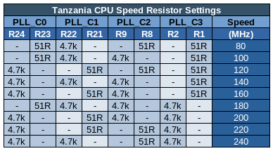
Resistor Settings for Various Speeds

Fitting a Header

If you instead choose to fit a pin header and use jumpers to set the speed, you will first need to remove the resistors and then the existing solder from the footprint. To remove the resistors, I put a large blob of solder on the tip of my iron and used it to heat both sides of the resistor at once and brush them off the pads one at a time. To clear the solder filled through holes, I’d recommend using flux and solder wick (aka solder braid). I’d set my soldering iron to about 350°C, paint on some liquid flux, wick out some solder while not keeping the iron on a pin hole for more than about eight seconds at once, and always lift the iron and wick off at the same time to avoid the wick sticking and potentially causing damage.

If the solder doesn’t clear, try again from the other side. If it still doesn’t, add a little fresh solder and try again.

That is the tricky bit. Once cleared, solder in a 6×2 2.54mm pitch header, or two 6×1 headers.
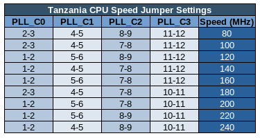
Jumper Settings for Various Speeds

The following representations show how jumpers should be fitted for a few common speeds.
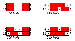
Note that the difference between 160MHz and 200MHz is only a single change, which is why, as mentioned previously, if you remove resistor R1 and then bridge pins 10 and 11 (for example with a blob of solder), your machine will be speed bumped to 200MHz from 160MHz, as long as it is able to run at 200MHz (the increase is 25%, which in general terms is quite a big speed increase for an overclock, especially without extra cooling).

Results

I removed the four resistors and cleared out the solder from the holes.
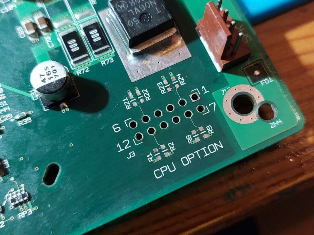
Then I soldered in a header, and fitted some green jumpers in the arrangement required for 240MHz. Reassembled my computer and powered it on.
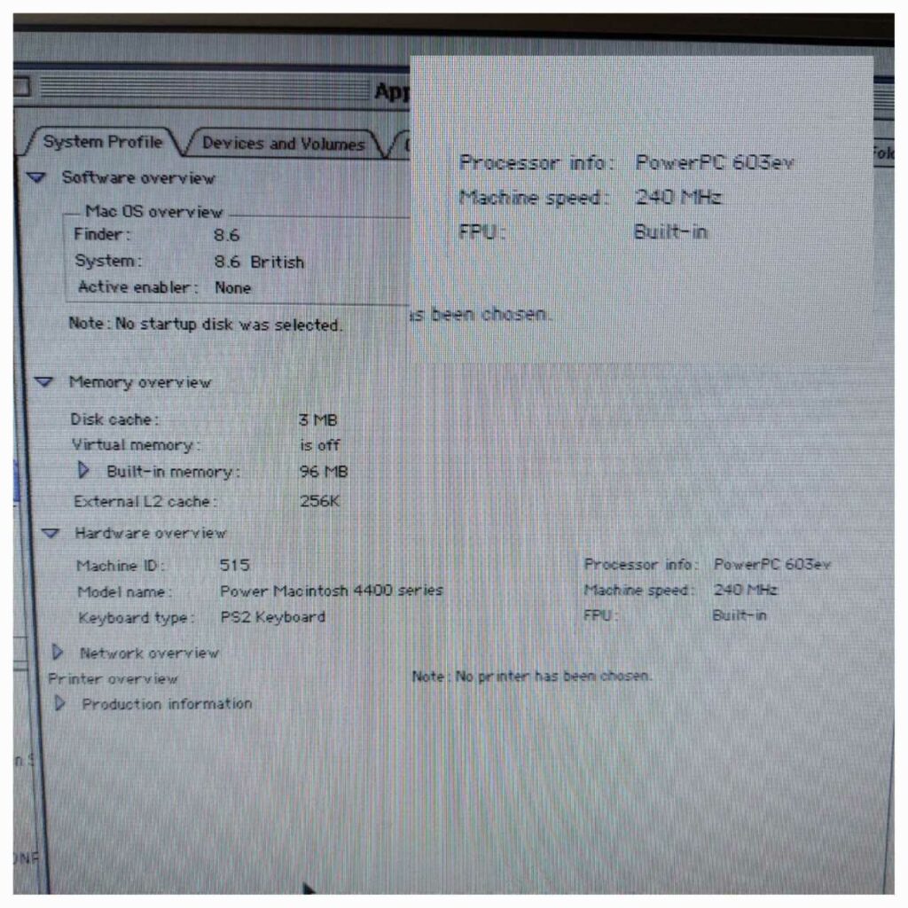
It booted happily and Apple System Profiler (in Mac OS 8.6) reports the CPU as a 240MHz 603ev, which is what was expected.
I ran some CPU benchmarks with the computer set to 240MHz and 200MHz (in that order, by powering down and swapping the jumpers around – I’d forgotten to get the “before” benchmarks) with Norton System Info from Norton Utilities 6 and got an 11% increase in the overall CPU score from the 20% overclock.
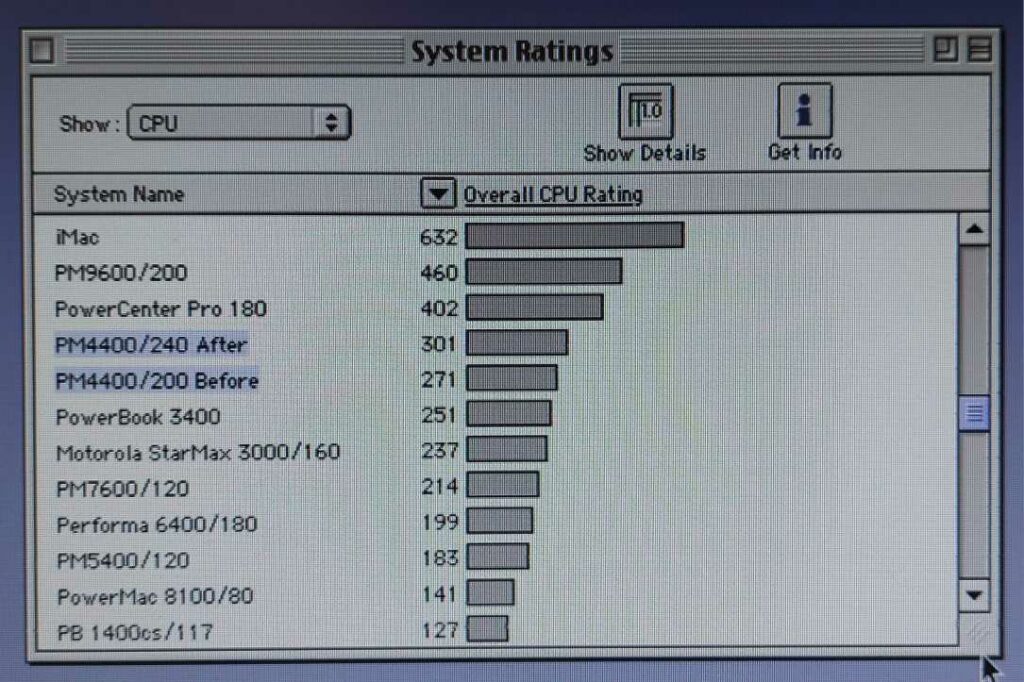
Looking at the detailed breakdown, we can see that tests that heavily use the RAM scored less well, with very RAM intensive tests seeing almost no change, moderately RAM intensive tests showing intermediate improvements and things like multiply and divide showing the full 20% uplift.

(Click to View)

I checked through the other benchmark categories (Video, Disk and FPU), Video saw almost no change, likely because most actions are been undertaken by the built in ATI mach64 video chip, with the exception of Ovals and drawing images, which I assume are both dependant on the CPU. Disk saw no significant change (except for random write, which I don’t fully believe and so am going to assume was due to a hiccup during the 200MHz benchmark).

FPU scales almost exactly with clock speed as usual, so we basically see a 20% uplift across the board.

In my specific machine, the CPU heatsink is cool enough to comfortable touch (indefinitely) while overclocked to 240MHz, even with the stock heatsink. Interestingly at 200MHz the heatsink is actually cool to touch, it cant be much different in temperature to my hand. I feel like with a bigger heatsink this computer would have a lot of overclocking potential, although I’m already at the maximum speed in the table.

Upgrading to a 604e

The board is technically able to use either a 603e (/ 603ev) or a 604e BGA chip. To do this, you would have to at least adjust the CPU core voltage by changing components in the voltage regulation circuit near the speaker connector. You almost certainly would also have to change some other resistors on the board as this is usually the case. Unfortunately as I don’t have the schematics, I don’t know what or where these would be.

It may be possible to meticulously compare a 604 based board with a 603 board to document the differences, but I don’t envy the individual that does that. A good place to start is probably at the “CPU ID” header, which also seems to be surrounded by four strap resistors.
CPU ID Header

If I remember correctly, the Performa 6400 schematics are available, and this is a sort of similar machine in some ways, so probably contains some clues regarding changes needed to fit a 604 to a machine that shipped with a 603. The Beige G3 schematics might also help as the design includes allowances for the 603 and 604.

Bus Speed

I’ve not done any investigation, but glancing at the board, it looks like the chips “U10” and “U11” are clock sources. The “U10” style of clock is usually set to one of several speeds based on resistors on some of the pins, but given its location, it might be controlling something in the chipset as “U11” has a 40MHz clock and is closer to the CPU. U11 looks like a shift register – I’m not sure what the circuit is doing exactly. I’d have to look into it, but hopefully these comments are a helpful starting point for someone else.

An old 68kmla post with a dead link mentions a need to move a resistor from R29 to R28 (next to the VRAM slot). But I don’t know anything about that. Well, it actually says the reverse, but mine is already like that, so I’m assuming they got it backwards, or perhaps my machine is already set like that. Sadly the website they’re referencing didn’t get archived by the wayback machine.

Update – Good news, I seem to have found an archive of an alternative version of the page in question here : http://web.archive.org/web/20040120030611/http://home.t-online.de/home/andreas.kann/44002.htmlhttps://68kmla.org/bb/index.php?threads/tanzania-to-tanzania-ii-upgrade.34251/

Further information is that they had trouble with the rating of their L2 cache… The good news is I have a 50MHz cache from my 6500!

Looks like I just need to find myself a 50MHz crystal.
Making a Wombat Fast

Making a Wombat Fast

Or, how to bump your Centris 650, Quadra 650 or Quadra 800 to 40 MHz with minimal effort.

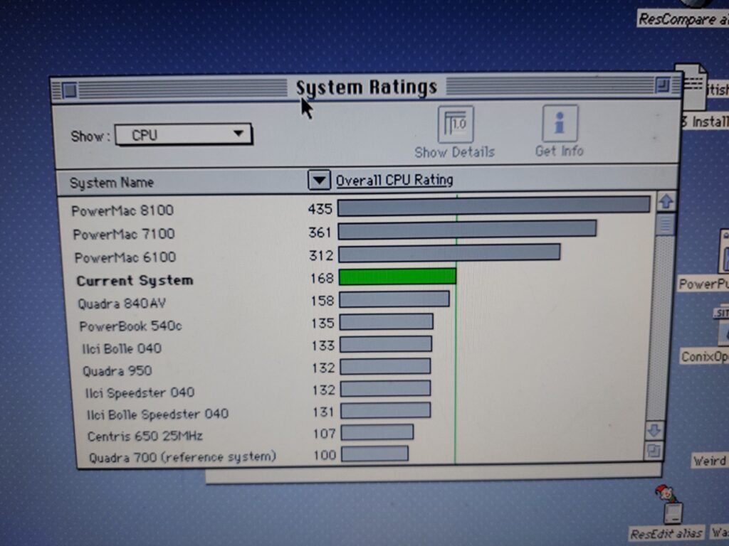
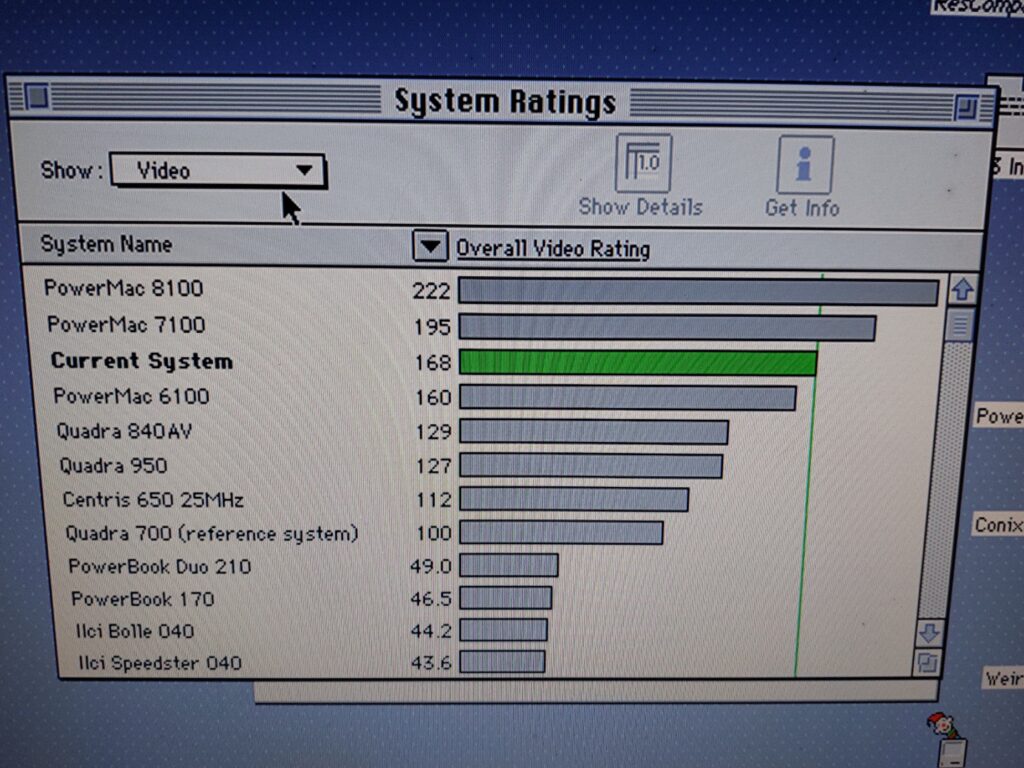
A 40 MHz Quadra 650 (“Current System”)

Traditionally, the way we have overclocked the Wombat family of Macs (the 650s and the 800) is to desolder the CPU clock “G3” and replace it with a faster part, or alternatively, use a commercial product that “clips” onto the clock, disables it, and injects its own clock signal. Through a mixture of experimentation and, let’s be honest, the sudden availability of the schematics, I made the most awesome discovery, I’ve found that 40 MHz is easy without messing with the clock. This is great news, because…
  • The clock is a surface mount part, meaning if you want to swap between speeds, you need to make a socket / adapter.
  • The clock is right up hard against a NuBus slot meaning you have to be very careful when desoldering and soldering in the area.

It actually turns out that the logic board in these machines has a built in function that lets you select the clock source, either from G3, or a clock derived from the NuBus clock. Selecting the NuBus clock as a source just straight up runs your computer’s bus at 40MHz without having to do any particularly fiddly mods.

There are a number of “levels” of effort you can put in, each with different advantages and disadvantages. You can either just hard set your computer to 40MHz and overclock in terms of the timings (because the ROM still runs with 25 or 33MHz timings), change the timings to the correct ones for 40MHz by swapping resistors, or by adding an extra resistor and two jumper headings, make it that by just removing or fitting two jumpers, you can select (independently) the RAM/ROM/VRAM timings and the CPU clock speed (between either 20 and 25 MHz, or between 33 and 40 MHz).

Basic 40 MHz Overclock

This is the simplest overclock with the minimal effort.

Advantages – This is effectively an overclock, so you’ll get super fast video performance as well as fast RAM and ROM.

Disadvantages – This uses whatever timings you already have, so almost certainly be unstable if you have a machine that shipped as 25 MHz, and possibly unstable if you have a 33 MHz machine.

How to do the Basic 40 MHz Overclock…

  1. Remove the logic board from your computer and place it on a heat-proof and static safe surface suitable for soldering.
  2. Find the pair of pads next to the CPU called “J29” on the silkscreen.
  3. Bridge the two pads, either with a blob of solder, or a little length of wire soldered between them. Alternatively, fit a two pin male header (2.54mm pitch) for a jumper.
  4. Reassemble your computer and test to see that everything works.
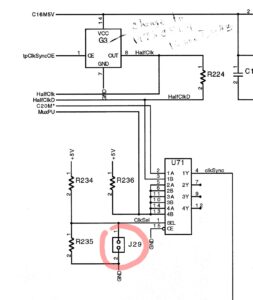
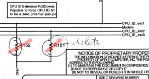
J29 on the Schematic

The modification works because U71 is wired to select between two clock sources depending on if J29 is fitted or not. As shipped, J29 is always open, ClkSel is always “high” and so the clock signal (half the bus speed) is always taken from G3. If you short J29, ClkSel goes low and the chip switches to using C20M – a 20MHz clock used by things like the SCSI and EtherNet chip, sourced from the NuBus circuit. Whichever clock is selected is doubled by the MC88916 chip before being fed into the CPU. Don’t worry that R235 isn’t fitted – it isn’t needed.

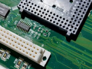
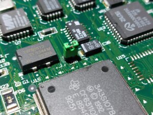
The Location of J29

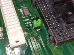
I recommend leaving a CPU in the socket while soldering to protect the socket from slips. In the photo above I’ve used solder wick / braid and flux to remove the solder that was in the through holes. You only need to do this if you want to fit a jumper (so you can select between the stock speed and 40 MHz by removing and fitting a jumper. The following shows my setup.

J29 with a Header and Jumper Fitted

If you don’t already have a CPU heatsink, consider fitting one.

Adding 40 MHz Timings

This is a more stable solution that requires a little more soldering. This mod is required if your computer originally shipped as a 25 MHz machine.

Advantages – This reduces the overclock on systems such as RAM, ROM and VRAM, likely making the system more stable at 40 MHz. Doing this change will make a 25 MHz machine work at 40 MHz.

Disadvantages – Benchmarks will score a bit lower than using 33 MHz timings at 40 MHz (in line with a real 40MHz machine if Apple had ever released one). The machine ID (gestalt) will change to an unreleased Mac – 7.6.1 will boot OK (but might not install without tricking the installer), but 7.1 won’t boot unless you can find a hacked System Enabler. (Update – I believe I’ve managed to make the required changes and have the magic System Enabler working now. Drop me a message and I’ll send you a copy).

How to select 40MHz timings…

  1. Remove the logic board from the case and place it somewhere suitable to do some soldering.
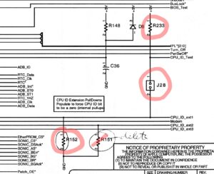
  2. If there is a resistor fitted to R152, remove it.
  3. If there is a resistor fitted to R151, remove it.
  4. Save any resistors in case you want to put them back.
  5. Reassemble your computer and test to see that everything works.
Setting 40 MHz Timings

The way I remove 0805 surface mount resistors is by putting a little flux on them, and then placing the iron on one end for about 3 seconds, before quickly moving the iron to the other pad and pushing the resistor off. Sometimes it takes a couple of tries, but it is easier than faffing with other methods and I usually already have my iron set up. It is especially helpful if there is plastic parts nearby on the board that hot air might damage.

The Ideal Setup

This last modification is closest (see the “Other Tweaks” section) to how I have my system configured as it gives the best flexibility. It lets you have jumpers to select CPU speed and timings. Removing both jumpers gives you the stock CPU speed (whatever it is on your machine), with (always) 33 MHz timings, while fitting both jumpers gives you 40 MHz and 40 MHz timings. You can also mix and match.

Advantages – Flexibility – you can change the CPU clock between stock (hopefully 33 MHz) and 40 MHz, and also the timings between 33 MHz and 40 MHz settings. All without even removing the logic board from the case (once the modification has been done).

Disadvantages – If you have a machine fitted with the original 12.5MHz clock for 25MHz, it will be slower than as shipped when you pick 25MHz by jumpers, because you will only be able to select timings designed for higher clocks.

If you have a 25MHz machine, I recommend just doing the first two mods above and basically hard wiring it to 40MHz. Make sure you have a heatsink fitted and consider finding a 33MHz grade CPU.

Dual Jumpers

To fit dual jumpers…

  1. Remove the logic board to somewhere you can do soldering.
  2. Make sure no resistor is fitted at location R151.
  3. Fit a 1.2k 0805 resistor (usually labelled 122) at location R152.
  4. Fit a 330 ohm 0805 resistor (usually labelled 331) at location R233.
  5. Fit a header at location J28.
  6. Fit a header at location J29 if you didn’t previously.
  7. Reassemble your computer and test to see that everything works.
J28 in Situ – This Selects 40MHz Timings when Fitted
R151, R152 (I didn’t have a 1.2k Resistor so used a 1.5k) and R233

At this point, as described above and if you started with a 33MHz board, you will be able to select 33 MHz with 33 MHz timings by removing both jumpers (I store them by placing them so they are on only one pin of the header), or 40 MHz with 40 MHz timings by fitting both jumpers. If you fit J29 and not J28, you will get a 40 MHz bus / CPU speed, with 33 MHz timings. This is an overclock with regards to the timings, so you will have boosted video, RAM and ROM performance. Most noticeable in the video benchmarks like the following :

Video Benchmark Score at 40 MHz with 33 MHz Timings

Note that while 40 MHz timings are selected, you will have the machine ID (gestalt) of an unreleased Mac, and System 7.1 won’t boot as mentioned above. If you want to boot in 7.1, just remove jumper J28.

Other Tweaks

  • Fit a 40 MHz Grade CPU and a heatsink.
  • Fit a socket for trying other clock speeds.
  • Fit a 25MHz clock to aim for 50 MHz.
  • Spoof a Quadra 800 power LED by shorting the appropriate two pins on the LED connector location. This makes your computer think it is a Quadra 800, which shipped with faster RAM, so I believe the ROM sets up slightly faster RAM timings.
  • Install the Wish I Were control panel to override the machine ID gestalt and reduce (but not completely) the number of issues from running a machine with an unreleased ID.
  • Replace the MC88916DW55 with an MC88916DW80 as this makes 50 MHz more likely in combination with a faster clock at G3. Fitting J29 still selects 40MHz, but removing it selects the faster clock at G3. Remember G3 is half the bus speed.
  • Remove onboard RAM and fit a single stick of very fast RAM (50ns EDO).
  • Fit a PowerPC Upgrade Card. Some will run at 80 MHz using the modifications described on this page.

I have personally done all the mods listed above to my machine, although I can’t promise they’ll all work for you, or are worthwhile.

Further Research

I worked out how to modify the System Enabler so that 40MHz works with System 7.1! Drop me a message if you want a copy. I might have previously posted it on Tinker Different – I forget.

Additionally, if your board shipped from factory with J28 and or J29 fitted, and especially R233 fitted, I’d be interested to hear from you. It’s likely that such a board would be a prototype and it would be great to check some component values.

This page is making a record of information I originally posted on 68kmla.

Overclocking the LC 475 in Software

Overclocking the LC 475 in Software

If you want to dive right in, it is recommended that you download and install the Control Strip Module version as this has the most up to date version of the software. The Control Strip Module version works in Systems from 7.1 through to 8.1, and supports overclocks in 24 bit addressing mode (my extension currently doesn’t). It also has better memory timings, and can often overclock slightly faster. It even has slightly different timings for the LC 475 and LC 575, to account for the difference in onboard memory speed. You can find a copy of the latest version on Macintosh Garden : https://macintoshgarden.org/apps/control-strip-475-overclock

The overclock is specifically designed to work with the stock 80ns RAM and VRAM in an LC 475 (etc.) And 70ns RAM in an LC 575.

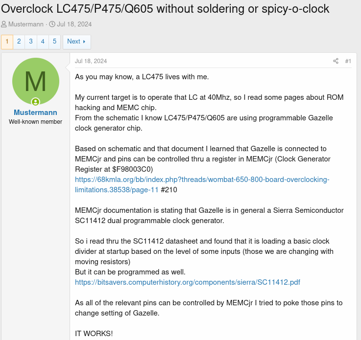
A little while ago Mustermann posted on the 68kmla forums that he was doing some experiments relating to overclocking the LC 475 without any hardware modifications. This was being achieved by controlling the LC 475’s programmable clock from the LC’s memory controller. The same process is possible on similar hardware such as the Q605 and LC 575.

Mustermann was kind enough to share his source code, and so zigzagjoe made an extension version for a fixed speed of 40MHz. Using Mustermann and zigzagjoe’s code as a basis, plus code from cheesestraw’s github, I started extending the functionality of the extension, including adding boot-time status icons, the ability to dynamically generate parameters based on a target clock speed and the ability to read instructions from the resource fork. I then made a control panel (actually a small application programme) to present user friendly interface for changing the extension’s settings.

An initial version apparently worked on some people’s 475s, but only allowed 20, 25, 33 and 40MHz on my own LC 475. After much digging, Mustermann was able to work out that I was providing values in an incompatible format to his magic sauce function that set the arbitrary speeds. This was fixed and now means I’m happy that the extension works as expected and so find enclosed the current version of the software installer :

Download Soft 475 Overclock

(Updated to Version 0.5.2 on 23rd October 2024)

The latest version, 0.5.2, is mostly identical to version 0.5.1, other than it contains a bug fix in the Advanced mode, where previously the Max and Min values were not being correctly saved.

Requirements

  • An LC 475, Performa 475, Quadra 605, Performa 476, LC 575 or Performa 577
  • Mac OS 7.5 or later.
  • Do not use this software if you have replaced the speed setting resistors on your logic board with blobs of solder. You really shouldn’t do this, and I don’t expect people have, but if someone has, it may cause damage (not limited to in conjunction with this software).

Optionally…

  • A heatsink for your CPU.
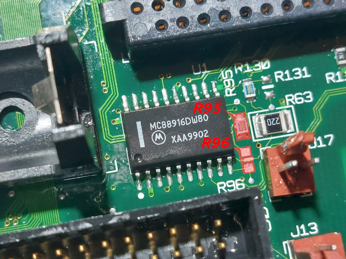
  • Move the zero ohm resistor at R96 to the R95 position to adjust the SCSI clock for 33MHz and above on LC 475 style logic boards. Not on the LC 575 type board, it already is set up for faster speeds.
  • A faster grade CPU.

Using the Software

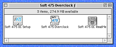
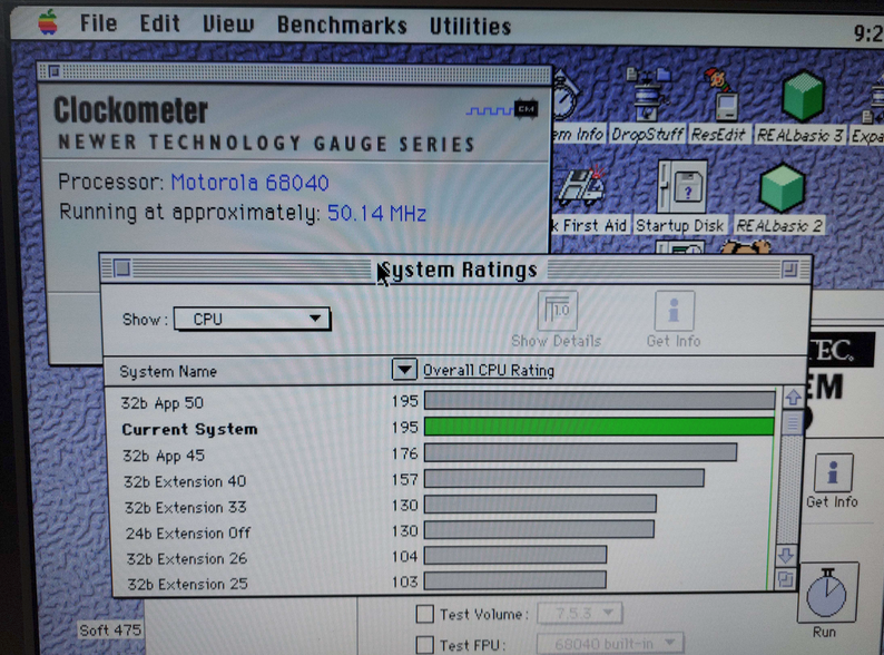
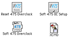
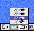
This .bin file contains an installer to run on your LC / Performa. It is pretty self explanatory. Once you’ve installed it, the software is “off” by default, so you’ll need to go to the “Soft 475 OC Setup” control panel and select what speed you want to try to run your computer at. This software will only work on the LC 475, Quadra 605, LC 575 and their Performa Equivalents. It may also work on the Apple STB. For an initial test, try selecting 33MHz from the menu, click “Set”, and then restart. Use Newer’s Clockometer software to verify the speed has taken. If this works, try 40MHz. If the computer crashes, or otherwise shows signs that it isn’t able to run at 40MHz, power off the computer, and power back on while holding the shift key to disable extensions. Once the computer has booted, use the control panel to set the overclock back to 33MHz or another speed known to work.

With some additional hardware modifications, namely changing the SCSI clock, replacing the clock multiplier with a higher grade chip and swapping in a higher grade CPU, I was able to get my LC 475 to run at 50MHz.

Selecting “Custom” from the “Select Speed” popup menu allows you to enter an arbitrary speed, recommended to be between about 20 and 40MHz, but depending on your exact configuration you might be able to go outside these bounds. You can enter fairly granular speeds, for example 37.6MHz, although Clockometer and other speed calculating software often isn’t accurate to this degree.

The “Advanced” option isn’t recommended unless you’ve read and understood the clock generator chip’s datasheet, but is there for users who want to exactly tweak parameters. Entering values in this dialogue box without understanding them will very likely just crash your computer.

LC 475 SCSI Clock Modification

For best compatibility while overclocking the LC 475 and other machines with the same logic board (not the LC 575 etc., which shipped with this modification as stock), it is beneficial to move the resistor located at R96 to the empty R95 position. This divides the SCSI clock by two and brings it back within specification. Note that this does not halve the performance of your SCSI bus. If you don’t do this modification, some people find that their computer crashes during large file copies, even at speeds as low as 33MHz. With this modification, the SCSI clock is within specification all the way up to 50MHz… if your computer still crashes, the issue is more likely your RAM (including onboard), VRAM or CPU grade. The good news is that all of these can be replaced with faster parts, although replacing the soldered RAM is a little tricky.

Potential Issues

When overclocking, sooner or later you will hit the limits of your hardware.

The first limit you reach is likely to be the SCSI clock on the LC 475 (not the LC 575, which is already set for higher speeds), meaning you’ll need to do the SCSI clock modification identified above. After that, you might want to fit a faster CPU, VRAM and RAM. Removing the RAM soldered to the logic board can help, and you don’t need to solder new RAM onto the board if you don’t want to, as long as you have a SIMM fitted. Remember the LC 475 can work with SIMMs up to 128MB in size, so the onboard RAM isn’t too critical.
I have also fitted an MC88916DW80 in place of the original XC88920 to hopefully improve performance at high speed. These can be bought from your favourite Chinese online retailer, although be cautious of re-labelled parts.
Once you exceed 40MHz, there will come a point at which you may have issues with the serial ports and floppy drive. I haven’t done extensive testing of this myself yet.

Note that most 25MHz 68LC040 CPUs will happily overclock to at least 33MHz, although it is always good to fit a heatsink. It is generally not a good idea to run an LC 475, and especially an overclocked one, with the lid off as the lid helps ensure airflow over the CPU and other components.

Future Development

Moving forward I’d like to add some more features and tidy up the user interface. Things I’d like to add include…

  • On the fly clock speed changes.
  • Estimated current speed display.
  • Holding numeric keys during boot sets predefined clock speeds.

Coming Soon… Cancelled

Version 0.6 was undergoing testing and has some cool new features, including the ability to set independent speeds for your 68040 and PPC601 if you have a PowerPC upgrade… which I don’t.

1728563016567.png
  • On the fly clock setting.
  • Independent speeds for 68040 and PPC.
  • Built in speed estimation.
  • Hopefully improved user interface.
  • Included speed change XCMD for use in your own projects.
  • Reduced file size for easy install from 800k floppy disks (possibly even 400k, depending on how much formatted space they have).
  • Technical improvements to ensure you don’t accidentally run the wrong control panel with the wrong extension.
  • A shutdown item that sets the speed back to the default for your computer, or you could just leave it on your desktop to reset to the baseline frequency manually.
  • Some pretty icons.
  • A visual indication of whether you are currently booted as a 68k or PPC Mac.

Sadly I’ve been unable to get the PowerPC upgrade specific code tested, as multiple months have passed I’m moving on from the project.

However…

… I made a Control Strip Module which allows on the fly speed switching (i.e. without needing to restart). I found this very helpful template to use.

The control strip module can be downloaded here. https://macintoshgarden.org/apps/control-strip-475-overclock

Thank you to the author of CSShell for permission to release it.

Feedback

Please let me know if this software works well for you. The github project can be found here the actual download for the software is near the top of this page and you’ve scrolled past it. Feel free to use the software as the basis of your own projects.

Upgrading My Acorn A3010

Upgrading My Acorn A3010

I also made this page, to help someone install the DualClock board in their A3010.

Background and Repair

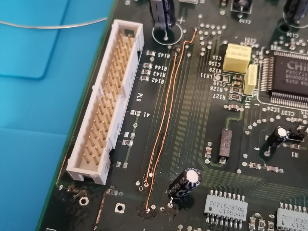
Battery damage repairs – Thankfully the floppy port was OK

I don’t remember exactly when, but at some point around 2000 my parents got me an A3010. I didn’t have any software for it beyond what was in ROM and didn’t really know anybody with an Acorn, so I basically just used it as a faster BBC Micro, especially as it had an Analogue / Userport podule in it and I was starting to get into electronics (slowly) during my later teens.

I used it intermittently for a few years, until I left home and couldn’t easily take it with me for the first few years.

Later, I had it in the house but hadn’t really done much with it other than test it once to check it worked. After that, I hadn’t used it for a few years when a collogue warned me that the batteries caused serious damage (in about 2014). I went home and pulled it to bits to find green corrosion and a dead battery. I cut the battery out and cleaned it as best as I could with IPA. The trace damage didn’t look like something I knew how to repair so I sadly packed it away hoping to work out what to do at some point. At least the battery was out of it.

The year : 2021 – the world is in disarray as a pandemic sweeps the earth and I had accidentally bought a dead, battery damaged Macintosh IIx… and was surprised to discover that it turns out I am now comfortable doing trace repairs. I’d also picked up an ultrasonic cleaner and decided to take the chance to clean up and have a look at the poor A3010. Looking at the board again, I found that it wasn’t as bad as I thought and a small number of trace repairs later and a clean, and I had it up and running. (Note that the traces to the parallel port are not in great condition, but do all conduct. I may return to tidy them up a bit at a later date, by re-tinning and covering with fresh soldermask).

Functional still… but ugly and in need of pre-emptive work

Upgrades

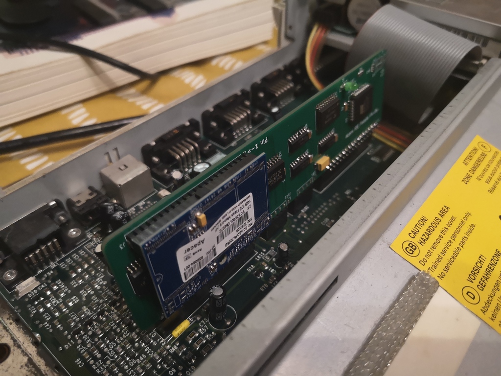
Excited to have a working Acorn, I decided to upgrade it to say sorry for abandoning it for years. I bought a Gotek, IDE card from IanS and 4MB of RAM. Further investigation found mentions of quite significant overclocks being possible, especially when using a fast 4MB RAM upgrade, as this disables the onboard RAM.

IDE Podule and 1GB DOM

Overclocking

The description of the overclock explained how, but not why this was possible, which made me a little uncomfortable so I decided to investigate. Why is it possible to overclock some (not all easily – some do not have the unpopulated footprint for an additional clock) A3010s by just adding an additional clock and a resistor?

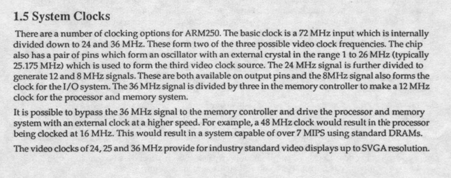
The following extract from the ARM250 datasheet was interesting as it describes the standard configuration for an A3010 – the 72MHz clock is divided by 2, and then again by 3, to produce the 12MHz for the processor and for the memory. The next paragraph then goes on to explain that it is possible to use an alternative clock source and even references running the chip at 16Mhz (with no warnings or statements that “this is not advised”).

ARM250 datasheet extract 1

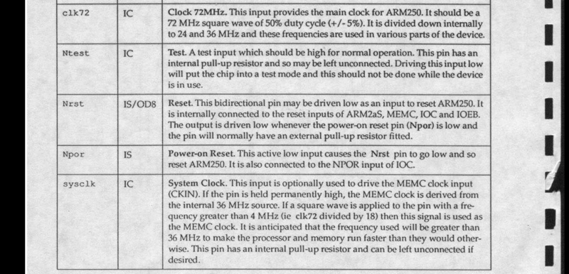
Further into the datasheet, there is a description of pin functions for the ARM250 that includes a description of “sysclk”. This is the optional input described above, and the description explains why this pin makes overclocking so trivial.

ARM250 datasheet extract 2

Apparently, the act of connecting an active clock in the correct speed range alone is enough to cause the ARM250 to automatically detect it, and switch clock source from clk72 (divided by 6) to sysclk (divided by 3). If no signal is detected and the pin is held high, it switches back to clk72. There is even conveniently a pullup on the pin so if left unconnected (as by default on the A3010) it is pulled high and disabled.

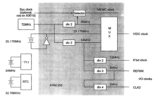
The following drawing also helps understand how everything works, showing how the chip is able to select from two sources, and where the dividers sit.

Diagram of ARM250 clock arrangement

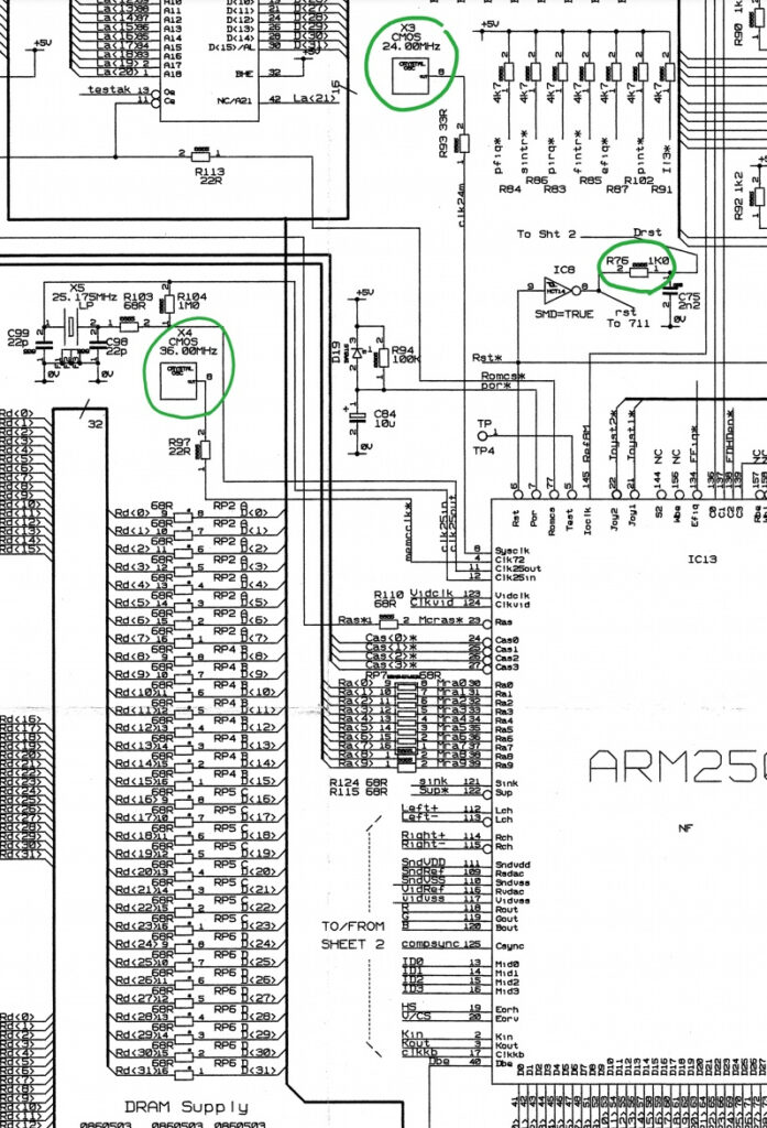
Next I pulled out various related schematics I had, some using sysclk and some only clk72. It should be noted that, firstly, the mezzanine A3010 is implemented in a slightly different way because they do not derive the clock by dividing by 6. Documentation states that this was done to avoid expensive clock dividers. Secondly, my A3010 is a later board revision and frustratingly does not match either schematic. The following is the mezzanine A3010 design. This variant uses sysclk, but it only implements a divide by 2. Note also that Clk72 is only 36MHz instead of the obvious 72MHz. This is due to the cost optimisation. Note that between the Clock X3 and sysclk a 33R resistor has been placed in line – make a note of this. Ignore that the mezzanine board is confusingly labelled “ARM250”.

Mezzanine A3010 clock circuit schematic extract

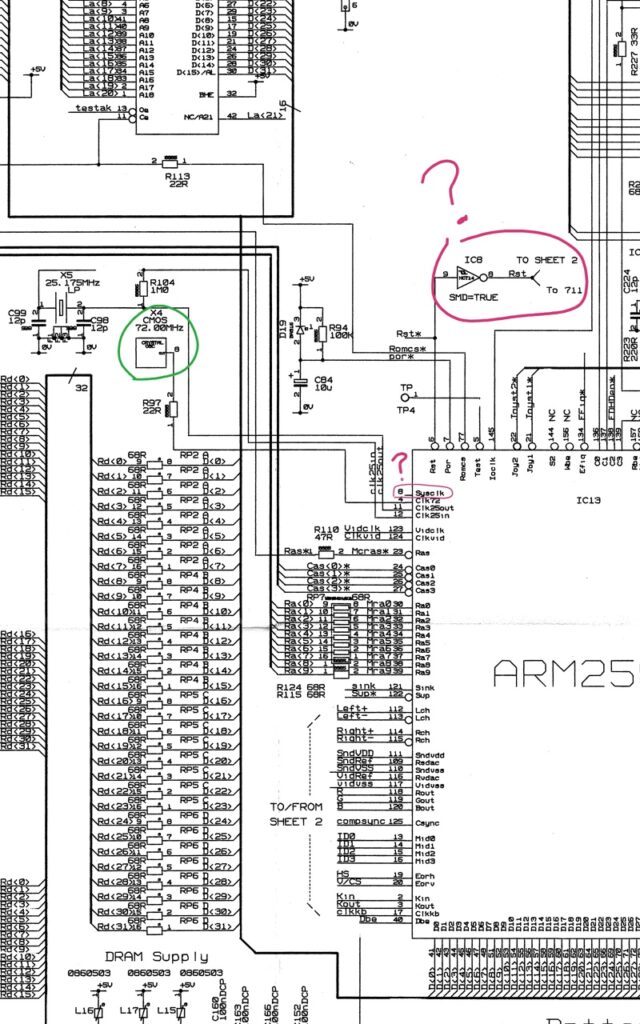
The following schematic extract is for the intermediate age A3010 which used the ARM250 chip rather than the mezzanine board.

ARM250 A3010 clock circuit schematic extract (early?)

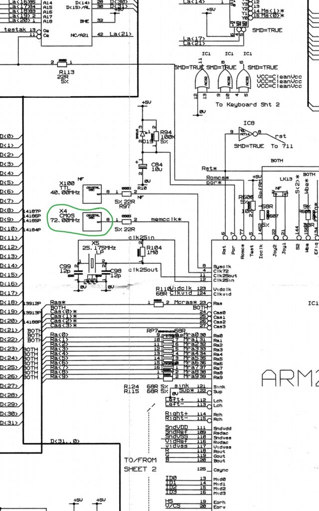
Here we can see sysclk is completely unconnected and X4, connected to clk72, is a 72MHz crystal showing that now, in line with the normal operation of the ARM250, the processor clock is one sixth of clk72. On boards of this design (with no footprint for a clock connected to the sysclk pin), modifications are still possible, but more complex. It would be necessary to tack a wire onto the processor pin, find ground and 5v and then wire in a resistor and a clock. Not impossible… but care would need to be taken.

Finally, the following is a schematic for the A3020. This schematic shows an implementation using an ARM250 (not a mezzanine board), but, with a position for sysclk.

A3020 clock circuit schematic extract (similar to my A3010)

Note two things here 1) while overclocking is likely possible by placing a fast clock at location X100, for a significant overclock I suspect it would be necessary to replace the RAM soldered on the motherboard with faster chips and 2) the clock shown in the schematic is 40MHz meaning that a machine built as above would be 13.3333MHz?! I anticipate that on machines that were sold, no clock was fitted at this location on the A3020, possibly confirmed by photos at BeebMaster and Chris’ Acorns.

The most interesting thing for me about this A3020 schematic is that this section more closely matches my A3010 than either of the A3010 schematics. Note here that the resistor located in line with the clock signal, between sysclk and X100 is in this case a 22R resistor. Given this schematic uses the same design as my A3010, I decided I would use a 22R resistor.

Using a 22R resistor contradicts the article on Vectorlight as they have used a 220R resistor – I suspect this was a result of confusion at some point. A surface mount 22R resistor is labelled “220” in this situation, the first two numbers are the significant figures, and the final number is the number of zeros. A 10k resistor would be 103 (ten and three zeros), so 22 and no zeros is 22R. I recommend that anyone following these instructions uses a 22R resistor. The footprint on the board is the size “0805” a bit small but not too difficult to solder if you use a bit of extra flux.

Implementing the Upgrade

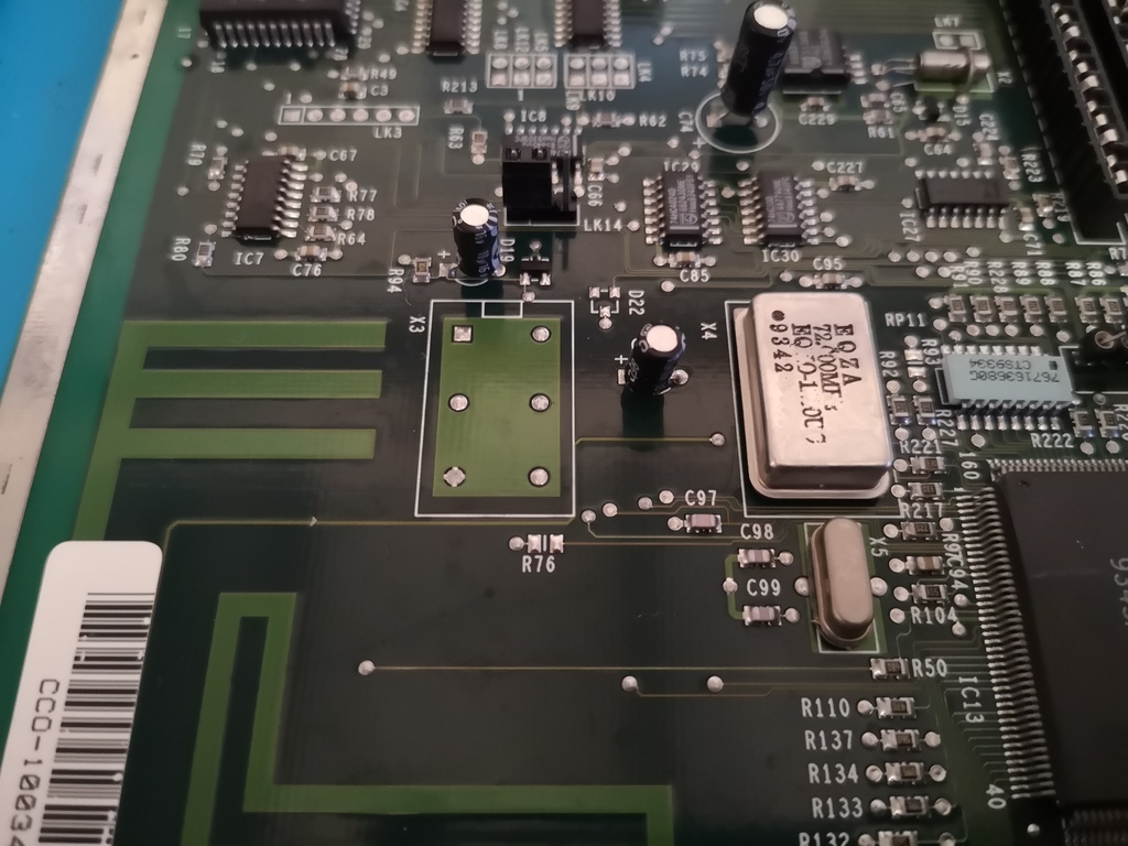
From the above, I now knew that I needed only two things – a DIP14 (or DIP8 – both work as the footprint supports both) style 5v output clock (TTL or a compatible CMOS etc.) and a 22R 0805 package resistor. To this, for convenience, I added a DIP14 socket, so I could easily swap in and out different speed clocks (“easily” I still have to half dismantle the computer, but at least I don’t have to keep desoldering clocks).

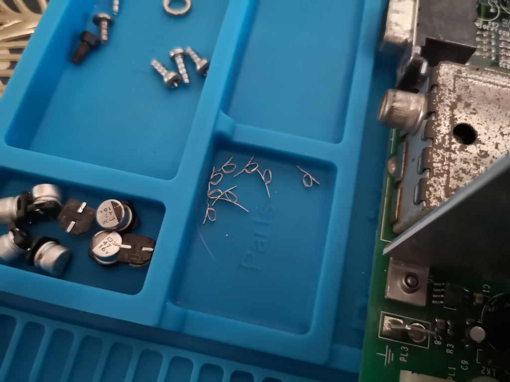
Removed socket pins (caps are from another project)

With the socket, I used a small pair of pliers to grab the 8 pins which were not needed and push them upwards. I then grabbed them from the top side and removed them. This left the socket with 6 pins in the locations matching the footprint on the motherboard. Note the notch on the silkscreen and on the socket as this tells you the correct orientation.

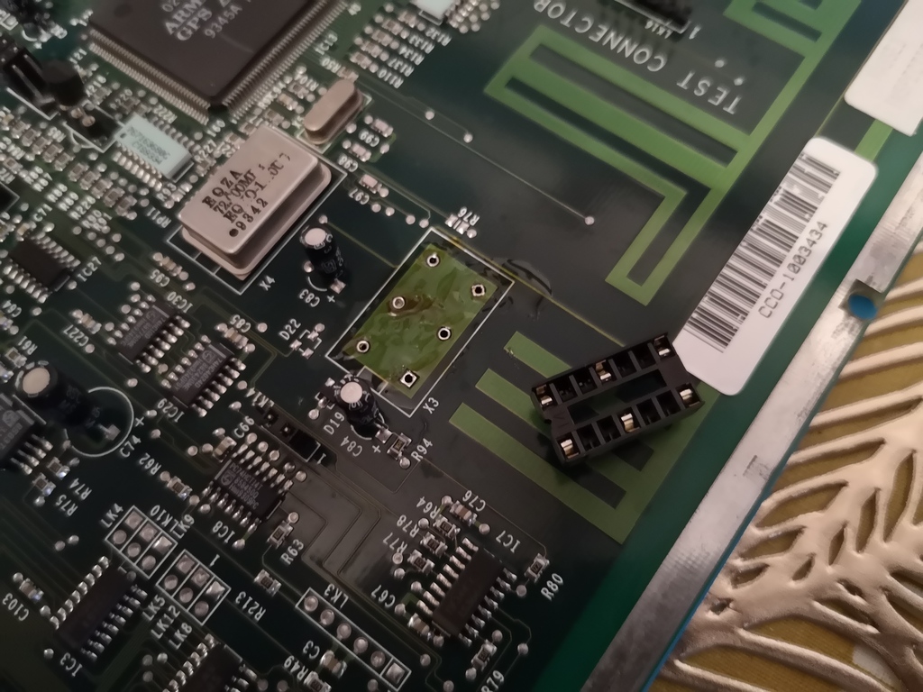
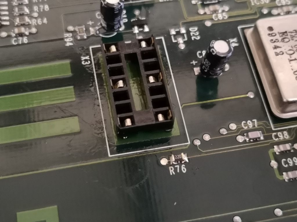
Solder mostly removed from X3 and the 6 pin DIP14

Next I used good quality solder wick along with some flux to remove the excess solder from the socket footprint for X3 (the location on my A3010 where the sysclk clock can be fitted). I find the best way to do this is to apply flux, add new solder and they use the solder wick to remove it. If it doesn’t all go (like the higher middle location in the photo above), try from the other side (after adding extra flux). If it still doesn’t clear, add more fresh solder (even though this is counter intuitive) and start again. Take your time and don’t keep your iron on the board for too long. Also, don’t set the iron too hot. Around 300 degrees C should be enough, certainly no more than ~330 degrees C.

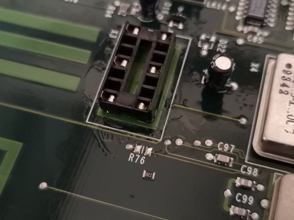
Socket in place in X3, R76 waiting to be fitted

Once all 6 holes have been cleared of solder, you can install the socket (taking note of the notch on the socket and on the silkscreen). I tend to tack one corner first, then with the socket downwards, place my finger on the socket and touch the iron to the single fixed pin so that it reflows and the socket sits flush on the surface of the PCB. Visually inspect before doing the same with the diagonally opposite pin… and if you’re happy it is installed properly, solder the other pins.

R76, a 22R 0805 resistor, soldered in place

R76 then needs to be fitted as above. First clear the pads of old solder using a bit of flux and solder wick. As mentioned, the 220 label means that this is a 22R resistor. To solder this, I place a small amount of solder on the pad closest to my soldering iron hand, and then briefly remelt this solder while using tweezers to push one end of the resistor into the solder and the whole thing into place. I then solder the other end, before applying a small amount of flux to each pad and reflowing them briefly to tidy them up. Don’t worry too much if it is scruffy, as long as the solder doesn’t bridge the two pads.

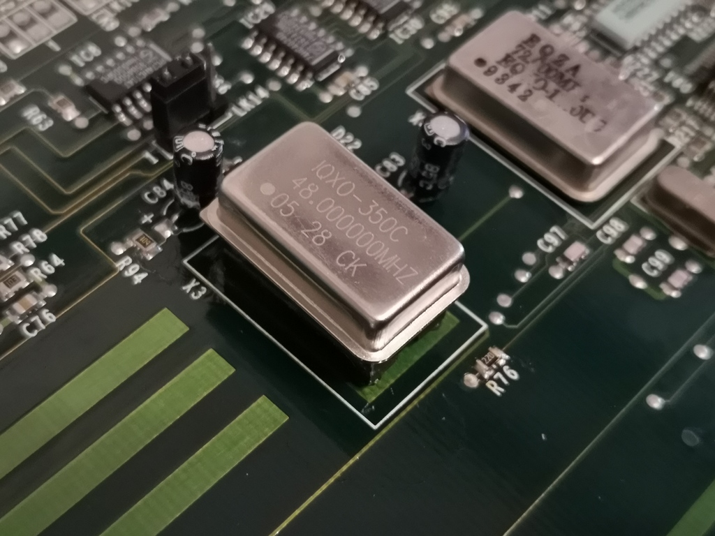
Ready to go – this 48MHz clock causes the processor and RAM to run at 16MHz

Fit a clock into the socket, taking care to note pin 1 (shown above by a dot next to “05”) and align it at the end with the notch in the socket and silkscreen. Note that if you use a shorter DIP8 style clock, you need to make sure that pin 1 is in the same location as with the DIP14 part. This means that the clock would be at the far end of the socket from R76.

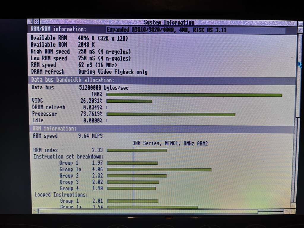
With the 48MHz clock above fitted, the A3010 ran at 48/3 = 16MHz, a 33.3% speed boost. I also later installed a 54MHz clock to give an 18MHz clock speed.

16MHz Processor and Memory

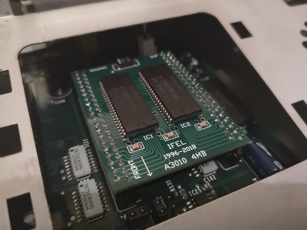
As I am using a RAM module rated at 60ns, 16MHz is within specification for the RAM, and 18MHz represents a very slight overclock (55ns).

IFEL 4MB RAM upgrade using 60ns chips

Note that interestingly, if you remove the clock and just leave the socket empty, your A3010 will return to its default 12MHz – this modification is trivial to “turn off”.

Turbo Mode

“DualClock” concept

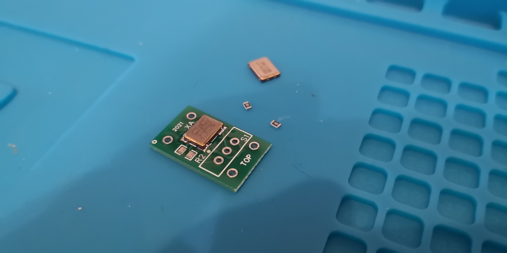
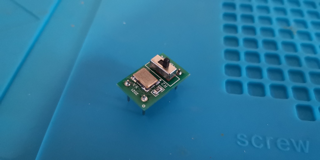
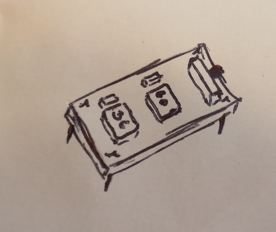
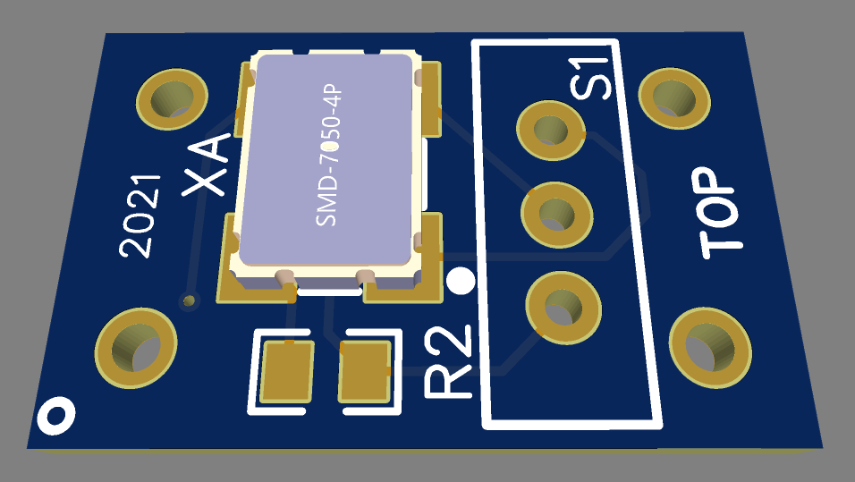
After having overclocked my Acorn, I started thinking. The DIP14 clocks are enormous, especially compared to more modern surface mount clocks that are functionally identical. I decided that I could probably fit 2 or 4 clocks on a small PCB that fit into the space envelope of the original part! A bit more investigating and I found that a commonly available 7x5mm clock package would fit one per side on a board the size of the standard clock package, with a SPDT switch (or header for a remote switch), allowing you to pick your clock speed.

Draft PCB Render

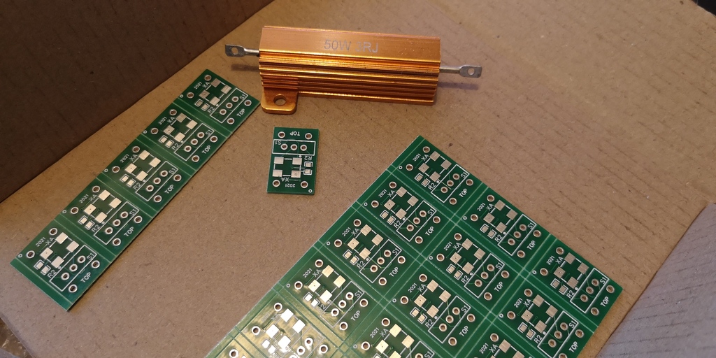
I created a schematic and board layout and ordered some boards to test the idea. A couple of weeks later they arrived and I made one up to test during my lunch break.

Bare boards – resistor for (unhelpful) scale
Under assembly
Complete!

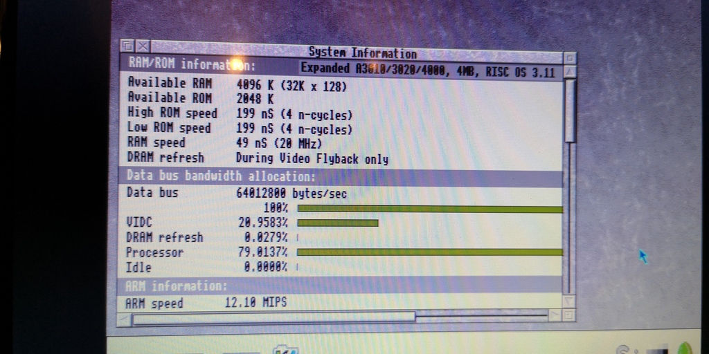
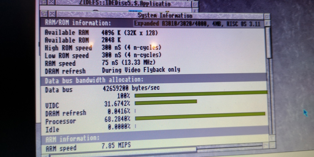
This test device is fitted with a 50MHz and a 60MHz clock, which results in a processor and RAM speed of 13.33MHz and 20MHz respectively, dependant on the position of the switch (in the current design, as photographed above, towards the camera selects the upper clock, and away selects the lower clock).

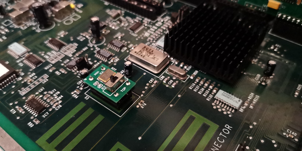
DualClock in situ (note the heatsink on the SOC)

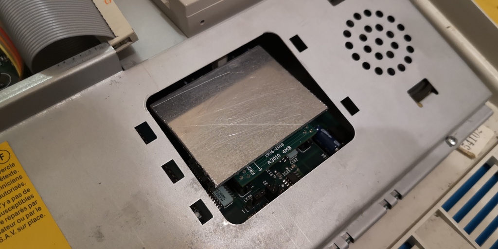
The excellent news is, it works! Note that by this stage I had fitted a standard 40x40mm heatsink. I also fitted a rectangle of aluminium to the RAM.

A crude “low profile” RAM heatsink

Both heatsinks were attached using a thermally conductive silicone glue, as I did not want them coming free inside the case.

Switch position 1

The photo above shows the A3010 running with the switch selecting the 60MHz clock and the following photo shows with the 50MHz clock selected.

Switch position 2

I do not advise switching the switch while the computer is running as it is likely that there will be some unpredictable states as the switch changes position due to switch bounce and the speed at which the two clocks respond. It is very likely that both clocks might be active at the same time and cause a crash.

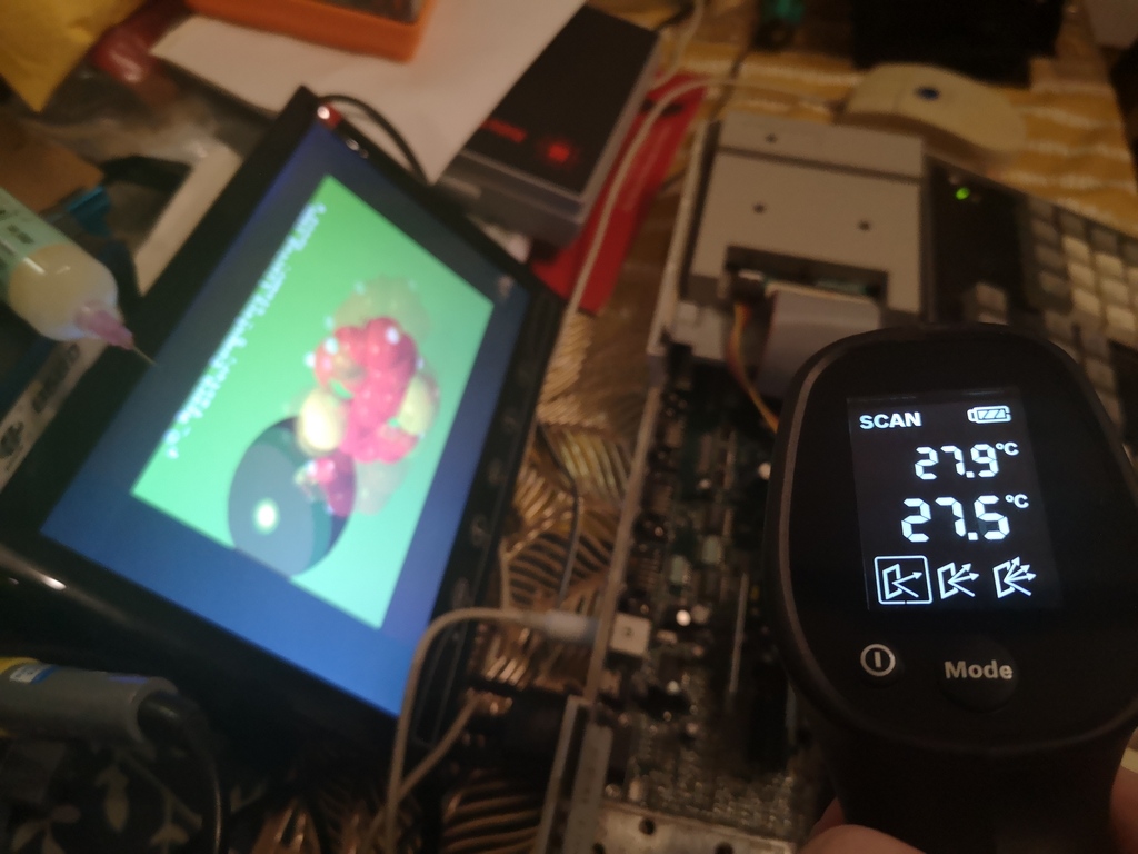
To test the 20MHz overclock, I left the Molecule example running at maximum (unrestricted) speed for over an hour. The SOC temperature peaked at about 29 degrees C (in the photo I’m not hitting the right place on the heatsink, down between the fins).

Measuring the temperature of the SOC heatsink

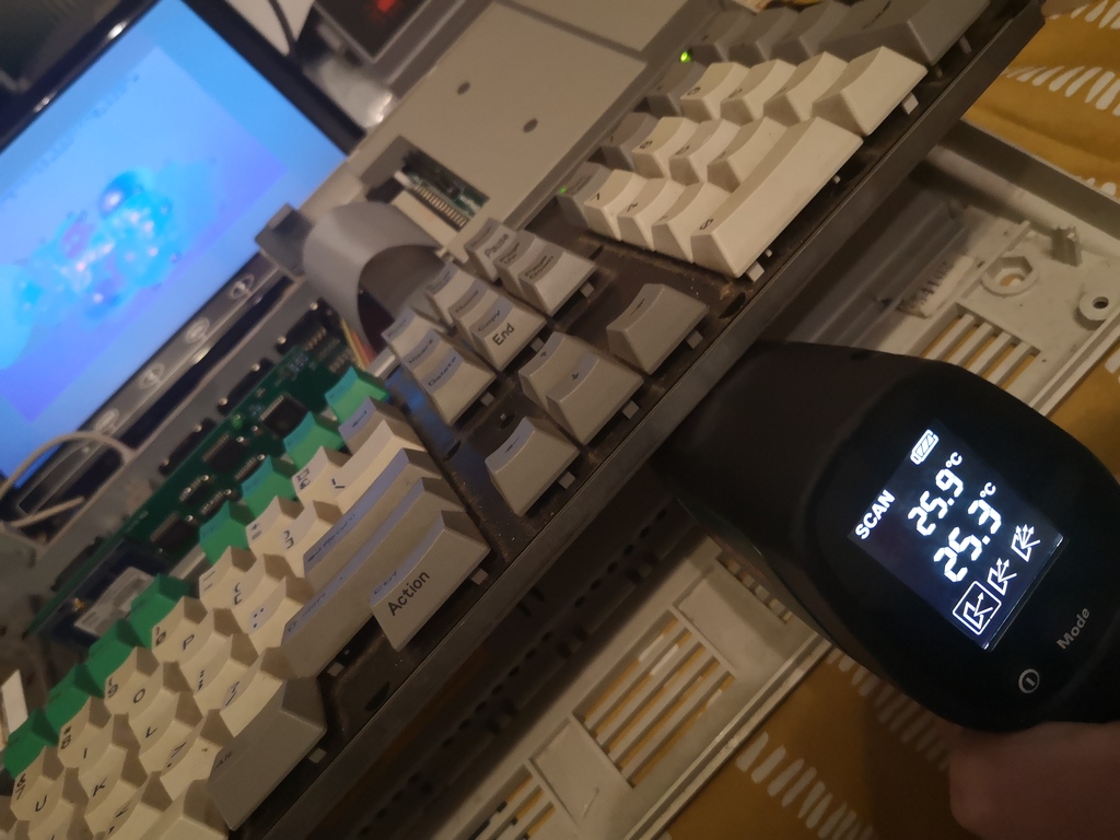
The RAM, to my surprise, was cooler at approximately 25 degrees C.

Measuring the temperature of the RAM heatsink

Next Steps

My intention is now to build a second PCB with a 60MHz and a 72MHz clock. This gives 20MHz and a 24MHz processor and RAM speed. My preference would be for 18MHz and 24MHz, but I don’t have a 54MHz SMD clock. With this PCB, I will attach flying leads and mount a three way switch on the podule blanking plate, with the correct wiring and switch, I’ve worked out that I can disable one, the other, or both clocks, giving me the ability to select 12, 20 or 24MHz. The best bit is that I wont have to keep dismantling my computer!

Stardot thread : https://stardot.org.uk/forums/viewtopic.php?f=16&t=21639